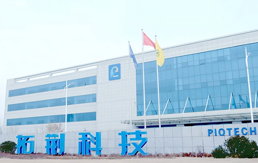
Tuojing Technology’s $3.3 Billion Capital Boost: The Quiet Battle for Semiconductor Equipment Scale-Up
Tuojing Technology raises capital by 3.36 billion yuan to expand production, seizing the opportunity for large-scale delivery of semiconductor equipment in response to the advanced packaging technology inflection point.
When Tuojing Technology, the domestic leader in thin film deposition equipment, increased the registered capital of its wholly-owned Shenyang subsidiary from 500 million yuan to approximately 3.36 billion yuan, this nearly six-fold capital expansion was by no means a routine internal financial transaction. At a critical juncture when advanced semiconductor manufacturing processes and advanced packaging are accelerating breakthroughs, such a massive capital injection directly signals that leading domestic semiconductor equipment manufacturers are moving beyond the early phase of small-batch sample validation and entering the deep-water zone of heavy-asset capacity expansion and competition for large-scale production line delivery.
Heavy Assets, High Barriers: The Ruthless Foundation of the Semiconductor Equipment Industry
The semiconductor equipment industry has always been an exceptionally brutal business defined by heavy assets and high barriers to entry. In integrated circuit manufacturing, thin film deposition, along with lithography and etching, ranks among the three core process technologies, directly determining wafer fabrication yield and line width. Over the past several years, the large-scale capacity expansion of domestic wafer fabs has driven the localization of semiconductor equipment, but for equipment companies, the real commercial consideration lies not merely in developing prototype machines, but in building the capability for high-standard, large-volume industrialized delivery.
An advanced deposition or bonding system is composed of tens of thousands of high-precision components. The upstream requires procurement of expensive RF power supplies, vacuum pumps, and high-precision robotic arms, while the manufacturing stage depends on ultra-high-cleanliness cleanrooms and extremely complex integration and testing production lines. As wafer fab orders are released in concentrated waves, equipment manufacturers lacking sufficient asset infrastructure to absorb massive inventory buildup and capacity expansion risk supply chain strain at any point during prolonged delivery cycles.
Capital Injection: Tuojing Chuangyi's Aggressive Strategic Intent
Tracing the evolution of this new entity through its underlying commercial blueprint, Tuojing Technology's strategic intent is decidedly aggressive. Business registration data from Tianyancha shows that Tuojing Chuangyi (Shenyang) Semiconductor Equipment Co., Ltd. not only saw its registered capital surge from 500 million yuan to approximately 3.36 billion yuan, a 572% increase, but also completed a change of legal representative from Liu Jing to Ning Jianping. As the core manufacturing vehicle wholly owned by listed company Tuojing Technology, its business scope, as disclosed by Tianyancha, precisely covers the manufacturing and sales of specialized electronic and semiconductor device equipment.
This multi-billion-yuan level capital increase essentially channels the parent company's financial strength directly into its northeastern manufacturing hub, building a super manufacturing fortress capable of handling production output worth tens of billions of yuan for next-generation thin film deposition equipment and frontier products such as hybrid bonding in the three-dimensional integration space.
Technology Inflection Point Driving Demand: The Urgent Need for 3D Integration and Advanced Packaging
The deeper driving force lies in the urgent demand for advanced packaging and three-dimensional bonding technologies created by the inflection point in wafer manufacturing technology. As Moore's Law approaches its physical limits, relying on chip stacking and advanced packaging to sustain computing power growth has become a shared path for global semiconductor giants. Core equipment for 3D integration imposes near-stringent requirements on mechanical alignment precision and surface flatness.
Tuojing Technology's positioning in this field requires not only continuous consumption of enormous R&D funding, but also the establishment of a fully enclosed system at its Shenyang base spanning precision component machining, cleanroom assembly, and full-machine factory acceptance testing. Sinking nearly 3.4 billion yuan into a physical manufacturing entity not only substantially enhances its ability to leverage large credit lines from banks and industrial capital, but also provides ample cash flow buffer for securing globally scarce core components.
The Second-Half Competition: The Advantage of Capacity Barriers and Scaled Delivery
In the first half of the domestic semiconductor equipment competition, the focus was on overcoming choke-point technologies and gaining entry through the doors of the first wafer fabs. As the market enters the second half, the competition shifts to who can operate stably on high-volume production lines with the most consistent yield and fastest delivery speed. Tuojing Chuangyi's multiple-fold increase in registered capital represents a heavy-duty offensive launched to seize the industrial high ground.
It sends a clear signal to the outside world: in this industrial breakthrough campaign centered on the computing power foundation, only by converting capital into tangible capacity barriers and scaled delivery capabilities can a company firmly secure the ultimate advantage amid the intense global semiconductor cycle competition.