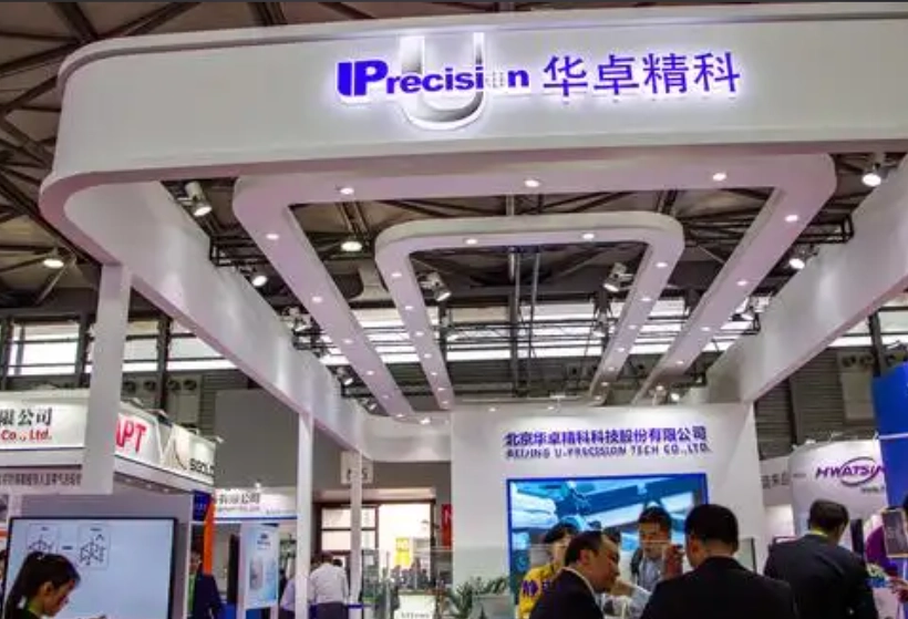
Huazhuo Jingke's $5M Move: The 'Ceramic' Sovereignty of Lithography Dual-Stage
Huazhuo Jingke establishes Ciyuan New Materials, focusing on core ceramic materials for lithography dual-stages, advancing the battle for semiconductor supply chain sovereignty.
In mid-2026, as the battle for localization of core semiconductor equipment enters full-scale hand-to-hand combat over foundational materials, the chips that determine the fate of top equipment makers are rapidly shifting from system integration down to micro-nano material sovereignty. Recently, Beijing Ciyuan New Materials Technology Co., Ltd. was officially established, with Sun Guohua, General Manager of Hwatsing Technology, serving as its legal representative. The company has a registered capital of 5 million yuan and is wholly owned by Beijing Hwatsing Technology Co., Ltd.
On the surface, an initial capital of 5 million yuan seems unremarkable in a semiconductor track where ventures typically require massive funding. The superficial consensus circulating in the industry is that this is merely a negligible shell set up outside the core business. Such shallow conventional wisdom completely overlooks the word that carries immense heavy-industry weight in the new company's name—"ceramics."
As a hardcore powerhouse that has conquered the core technology of dual wafer stages for lithography machines, Hwatsing's every move sends ripples through the most sensitive nerves of domestic semiconductor equipment. The dual wafer stage demands extreme lightweight construction, ultra-high rigidity, and zero thermal expansion coefficient in nanometer-level precision motion. At this technological inflection point where advanced processes push toward extreme manufacturing limits, precision advanced ceramic materials have become the only solution for supporting air-bearing precision motion stages to achieve high stability. Hwatsing's strategic positioning of Ciyuan New Materials at this moment is by no means blind experimentation—it is a supply chain sovereignty recapture campaign personally led by the General Manager.
The fact that Sun Guohua personally serves as the legal representative of this new materials entity—a highly contrasting top-level arrangement—completely betrays its strategic significance. According to industrial and commercial compliance data shown by Tianyancha, this new entity has already tightly cemented new materials promotion and software development into its business scope. This signals that Hwatsing is not only taking on the gritty work of new materials R&D but is also attempting to output a standardized ultra-precision motion base solution to the entire upstream of domestic wafer inspection and laser repair equipment through pixel-level alignment between software control algorithms and the physical properties of ceramic materials.
As for keeping the initial capital at 5 million yuan, this precisely reflects the seasoned asset planning of a hard-tech veteran. Advanced ceramic R&D is fraught with technical uncertainty. By using an independent legal entity as an incubator, Hwatsing not only isolates the financial risks of material trial-and-error with minimal capital erosion—preventing fallout on the parent company's income statement—but also positions this clean entity as a bargaining chip to flexibly bring in external industry funds for capital amplification once the technology matures and moves to mass production.
In this brutal cycle where true cash-generation efficiency and core control determine ultimate survival, equipment assembly plants lacking self-sufficiency in underlying materials will ultimately pay the most expensive exit bill at the material moats built by heavy-asset giants. Having completed this round of foundational material positioning, Hwatsing is now using its restructured supply chain shield to coldly calibrate the highest sovereign coordinates of China's core semiconductor equipment amid the advanced process wave.